Microfluidic chip manufacturing: Methods, examples, and practical advantages
Explore microfluidic chip manufacturing methods including soft lithography, molding, etching, embossing, and 3D printing for scalable product development.
Microfluidic chips play an important role in many life science and industrial applications, enabling advances in areas such as drug discovery, diagnostics, cell biology, materials testing, and automated fluid handling. While much attention is paid to chip design and application, how a chip is fabricated often determines whether a concept remains a prototype or becomes a reliable, scalable product.
Different fabrication methods serve different stages of development. Some prioritize speed and flexibility, others consistency and volume, and others absolute performance. Understanding these trade-offs is essential when moving from early experimentation to real-world deployment.
This article provides a high-level overview of the main microfluidic chip fabrication methods and highlights where each approach fits best across life science and industrial applications.
Soft lithography
Soft lithography using PDMS remains a popular choice in academic labs and early-stage life science research. It offers low upfront cost, excellent optical transparency, and rapid turnaround, making it ideal for proof-of-concept studies, microfluidic circuit prototyping, and exploratory experiments.
For biological research, PDMS allows quick iteration of channel designs and easy integration with microscopy and cell culture. However, its material limitations such as absorption of small molecules and drugs, oligomer leaching, and unstable surface hydrophilicity make it less suitable for quantitative assays, drug screening, or regulated workflows. From an industrial standpoint, PDMS rarely meets requirements for robustness or scalability.
Best suited for: Life science research, prototyping, early biological studies
Less suitable for: Drug testing, regulated environments, scaled production
Injection moulding
Injection moulding is the gold standard for large-scale microfluidic production. Once a design is finalized, it delivers unmatched reproducibility, durability, and cost efficiency per unit.
In life science, injection moulding underpins disposable diagnostic cartridges and consumables. In industrial microfluidics, it supports robust components integrated into automated platforms operating at scale. The key limitation is flexibility: high tooling costs and long lead times mean design changes are expensive and slow.
Injection moulding is therefore most effective when the design is stable and production volumes justify the initial investment.
Best suited for: commercial diagnostics, consumables, industrial platforms
Less suitable for: rapid iteration and early development
Typical materials: COC, COP, PMMA, PC
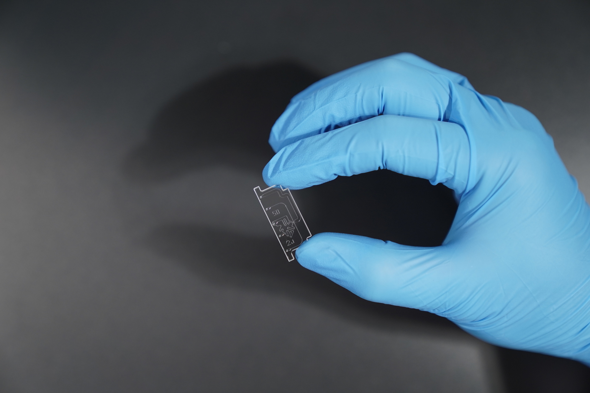
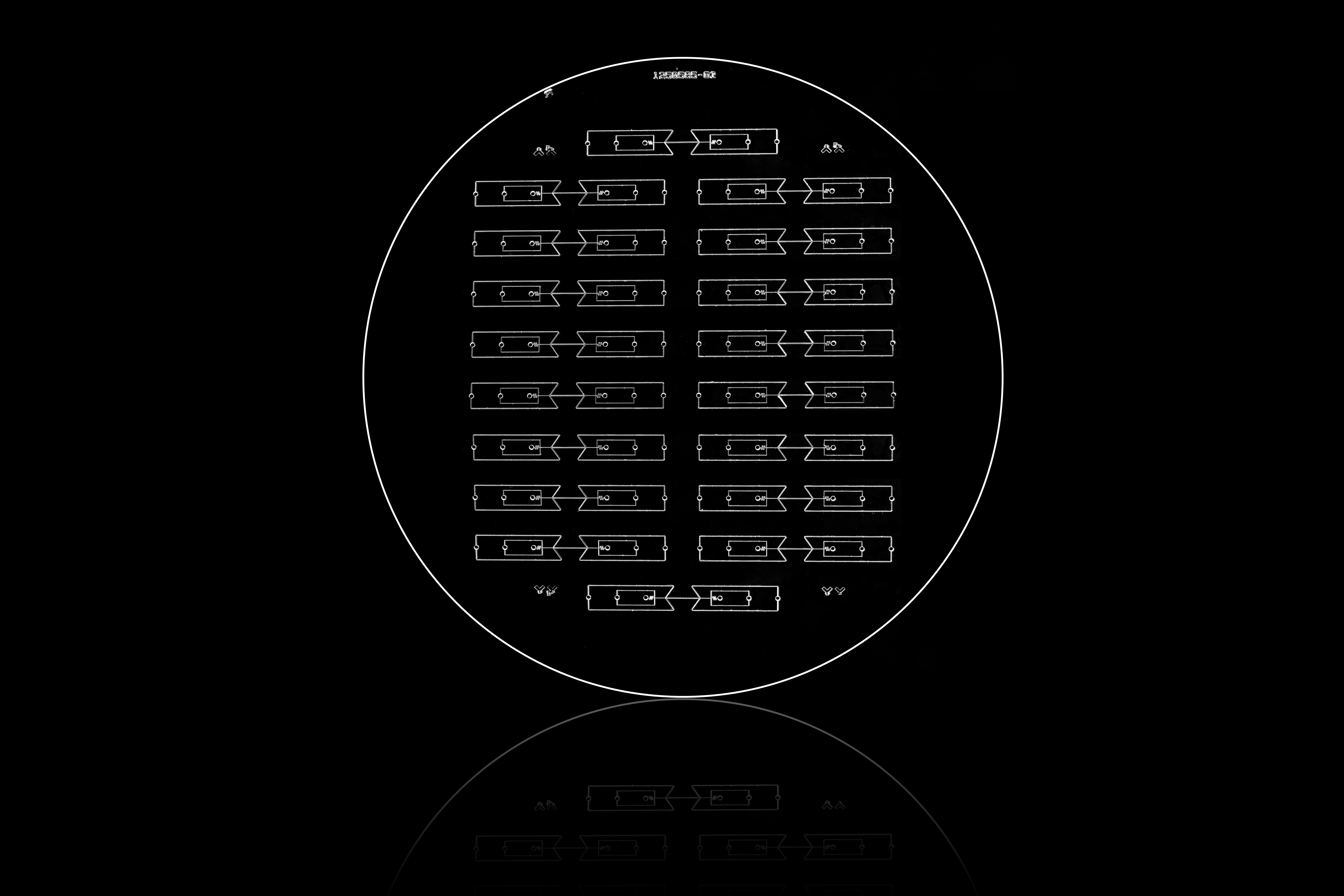
Etching
Etching-based fabrication is commonly used for glass and silicon chips. Techniques include wet etching, dry etching, and deep reactive ion etching (DRIE), enabling high-precision microstructures.
In life science, etched chips are used in analytical chemistry, advanced diagnostics, and applications involving aggressive solvents. In industrial microfluidics, etched devices excel in harsh environments where polymers may fail.
An example provider in this space is IMT Microtechnologies, which offers precision glass microfabrication for microfluidic and lab-on-a-chip systems. Standard photolithographic wafer-level processing, wet etching and laser structuring techniques are commonly used in this type of fabrication to produce well-defined microstructures, tight dimensional control, and consistent device performance. These approaches are particularly suitable for applications with high demands on optical properties, chemical resistance, mechanical stability, and long operational lifetimes.
Due to the well-established wafer-based processing technologies, glass manufacturing remains highly scalable. However, it still lags the efficiency of polymer replication methods. Etching processes are typically more complex and expensive than polymer replication methods, and throughput is lower. As a result, etched chips are best positioned for high-value, performance-driven systems rather than disposable or mass-market consumables.
Best suited for: analytical life science tools, high-performance industrial systems
Less suitable for: high-volume, low value consumable products
Hot embossing
Hot embossing provides a manufacturing middle ground between PDMS prototyping and injection moulding. It supports thermoplastics commonly accepted in regulated environments, while offering tooling costs and lead times that are typically lower than those of injection moulding.
A range of thermoplastic and elastomeric materials can be used with this approach, including polymers such as COC as well as newer thermoplastic elastomers. Depending on the material, these platforms may offer advantages over PDMS, such as reduced small-molecule absorption, minimal leaching, more stable surface properties, and the ability to form reversible or room-temperature seals without plasma treatment. These characteristics can simplify assembly and enable workflows that require repeated device access or sample recovery, such as tissue harvesting.
For teams transitioning from research to product, hot embossing provides a realistic path to scale without sacrificing performance.
Best suited for: Life science translation, pilot manufacturing, medium-volume production
Less suitable for: Very fast mass production, very complex 3D or overhanging geometries, high precision, materials needing high chemical/temperature resistance.
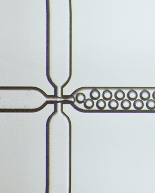
3D printing
3D printing has quickly become one of the most practical ways to accelerate microfluidic development when speed, flexibility, and design freedom matter most. Without molds, cleanrooms, or tooling, teams can move directly from CAD to a functional chip in just days, dramatically shortening development cycles and enabling rapid iteration.
One of the biggest advantages of modern microfluidic 3D printing is the ability to fabricate fully enclosed channels in a single build, eliminating post-processing steps such as plasma bonding, thermal bonding, or layer alignment. This not only simplifies fabrication but also improves reliability and reduces leakage risks. Unlike traditional layer-based methods that restrict designs to mostly planar geometries, 3D printing enables true 3D channel architectures—including vertical interconnects, complex routing, embedded features, and curved paths that are extremely difficult or impossible to produce with lithography or embossing. For example, researchers have used additive manufacturing approaches to create microvascular-like networks and models of vasculature, with interconnected channels that better mimic the branching structures found in biological tissues, facilitating applications such as organ-on-a-chip and perfusion-based studies.
Rapid Fluidics stands out in this space as a dedicated microfluidic technology provider rather than a general 3D printing company. Their platform is specifically optimized for fluidic performance, optical clarity, and high-resolution channels, allowing researchers and engineers to create functional, application-ready devices—not just structural prototypes. The ability to quickly customize designs, test multiple iterations, and directly manufacture sealed chips makes Rapid Fluidics particularly attractive for fast-moving R&D environments.

In life science, 3D printing supports early assay development, exploratory research, and rapid validation before committing to large scale manufacturing. In industrial microfluidics, 3D printing supports rapid feasibility testing, internal tooling, and validation of fluidic concepts prior to transition into injection moulding or hot embossing. While surface roughness, resolution limits, and material properties still constrain 3D printing, platforms like Rapid Fluidics play a critical role as a bridge between concept and scalable production.
Best suited for: rapid prototyping, custom designs, early validation
Less suitable for: high-volume or regulated mass manufacturing
Comparison of microfluidic chip fabrication methods
From concept to commercial reality
Successful microfluidic development rarely relies on a single fabrication method. Life science teams often start with PDMS or 3D printing for rapid iteration, then transition to thermoplastics or glass as assays mature and move toward validation or production. Industrial teams typically prioritize robustness, reproducibility, and scalability from the beginning.
At Blacksheep Sciences, we help teams navigate these choices by selecting the right chip technology for each application, designing optimised microfluidic devices, and advising clients on the transition from prototype to production. By combining scientific insight with engineering expertise, we support a smoother scale-up process, reducing risk, controlling costs, and accelerating the path from concept to real-world impact.
.png)
.gif)